
Image Stabilization
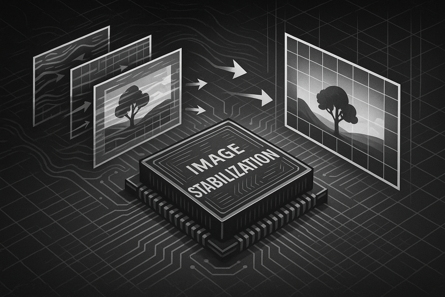
The Image Stabilization core is a full featured core that removes jitter from an input image.
An Image Stabilization behavioral model and simulation environment is also provided to the designer for simulation/verification of the Image Stabilization design in the system. The core employs multiple Vector Projection Correlators (VPCs) to calculate frame to frame movement vectors. The VPCs operate on regions of interest (ROIs). The VPC output is filtered to create an effective frame image. The shifted effective frame is then combined with the previous frame to create a reduced-jitter image.
Software driver examples and support are available to accelerate application development.
Feature Summary
- Supports color and monochrome images
- Uses DDR memory to support up to 2048 x 2048 images
- Native AXI4 interface to DDR
- AXI-Lite CPU-to-register interface
- Parameterized inputs (frame dimensions, etc.)
- Uses Local Area Processing (LAP) filter separates low- and high-frequency image components; used to create feature map
- Low latency (~ 1 frame)
- Input and output in the YCbCr color space
- Provides a general-purpose video bus, using DDC’s Common Video Format (CVF), simplifying interconnection of multiple video processing modules.
Resource Utilization
The Image Stabilization core is not limited to any vendor specific implementation. Versions are available for all major FPGA vendors, and can be created for any custom ASIC application. The following table shows typical resource requirements for an implementation.
AXI Image Stabilization 8-bit color – AMD Utilization Report
| Family | LUTs | FFs | MULTs | BRAMs (18K) | BRAMs (36k) |
|---|---|---|---|---|---|
| Virtex 7 | 3928 | 5266 | 5 | 7 | 10 |
| Virtex Ultrascale | 3908 | 5245 | 5 | 7 | 10 |
AXI Image Stabilization – Altera Utilization Report
| Family | Config | ALMs | FFs | LUTs | BRAMs (20K) | DSPs |
|---|---|---|---|---|---|---|
| Agilex 5 | 8-bit color | 3598 | 6360 | 5113 | 27 | 3 |
| Agilex 5 | 8-bit monochrome | 3522 | 6046 | 5024 | 20 | 3 |
Functional Description
The Image Stabilization core consists of five major blocks: feature generation block, VPC, motion filter, frame filter, and register file.

Figure 1 – Image Stabilization Block Diagram
The external CPU accesses the Image Stabilization core through an AXI-Lite 32-bit interface. All internal registers and data buffers are provided through this interface.
The input image to the image stabilization is sourced by a video lineup. The input comprises previously processed video via other video intellectual property (IP) components, e.g. non-uniformity correction, in the lineup.
The input image is converted to a feature map image and then passed to the projection-based motion estimator. Generally, motion estimates from several regions will be generated. The horizontal and vertical motion estimates are individually passed through a median operation to create the actual motion estimate. In order to accommodate intentional panning and motion, the actual motion vectors are filtered to create the effective motion estimate. This estimate is passed to the motion compensation block where the stabilized output frame is assembled.
In parallel, the processed input video is written to a DDR memory buffer, to implement a frame delay.
The stabilized video is also stored in DDR prior to motion compensation reassembly.
Memory access is implemented by two AXI4 buses (m00 and m01), which are mastered by the Image Stabilization core.
The core output is stabilized, i.e. jitter-reduced, video.
Feature Map Creation
Some video sources produce low quality output which makes the use of projection based motion estimation unreliable. In order to address this problem, the video is pre-processed prior to computing the projections. This pre-processing stage creates a feature map image which is then passed to the projection based motion estimation block.
Clocks and Reset
The Image Stabilization design is fully synchronous to the pixel clock (clock). The design uses a main asynchronous active low system reset (rst_n).
The pixel clock is used by the design to drive the main controllers, interrupt controller, and processor interface. The core has been proven in multiple designs at 40-50 MHz pixel clock rates. The clock rate should scale significantly higher, in FPGA implementations, with no stress on synthesis/place and route tools.
The AXI4 clocks (m00_axi_aclk and m01_axi_aclk) are used by the design to drive read and write accesses to DDR memory. The AXI4 accesses are tightly coupled to processing at the pixel rate; thus, clock domain crossings are eliminated by driving these clocks from the pixel clock.
The AXI-Lite clock (s_axil_aclk) is used only for register file accesses. The core implementation provides for an independent AXI-Lite clock port, but in practice this port is connected to the pixel clock, as well.
Each clock has an associated reset, active low.
Further details are available in the User Guide.
Testbench
The Image Stabilization Core comes complete with a unit level testbench. The testbench is fully automated and self checking.
The testbench can be used as a demonstration of how the interface is programmed by software.
Disclosure: The header image on this page was generated using AI.